Highlights
- Google’s Tensor G5 and G6 process upgrades leaked.
- Google Tensor G5 for Pixel 10 will be built on TSMC’s advanced N3E node.
- The Tensor G6 will be manufactured on TSMC’s N3P node.
It was previously reported that Google is switching to TSMC for its upcoming chips with confirmed reports that the Tensor G5 chip for Google Pixel 10 will be manufactured by the Taiwanese Semiconductor Manufacturer.
However, there wasn’t much update on which exact process would be used. Now we are getting reports about only on the Tensor G5 but also on the Tensor G6.
In an exclusive report, Android Authority has revealed important details from Google’s gChips division leak about the upcoming Tensor chips.
Android Authority confirmed of obtaining documents of the process nodes that will power Google’s future processors.
Google Tensor G5 To Be Built on TSMC’s Advanced N3E Node
According to the Android Authority report, the Tensor G5 is codenamed “Laguna” and is expected to be the chip in Google’s Pixel 10 series next year. It will be manufactured on TSMC’s 3 nm-class N3E node.
This is the same advanced process that was also used for Apple’s A18 Pro in the iPhone 16 Pro and the M4 chips.
This brings a significant leap compared to the previous Tensor G4 that uses Samsung’s 4 nm-class 4LPE node.
By switching to the N3E node, the Tensor G5 is set to bring massive upgrades in both efficiency and performance.
It is a promising development for Google’s hardware since this is considered the best process node currently available.
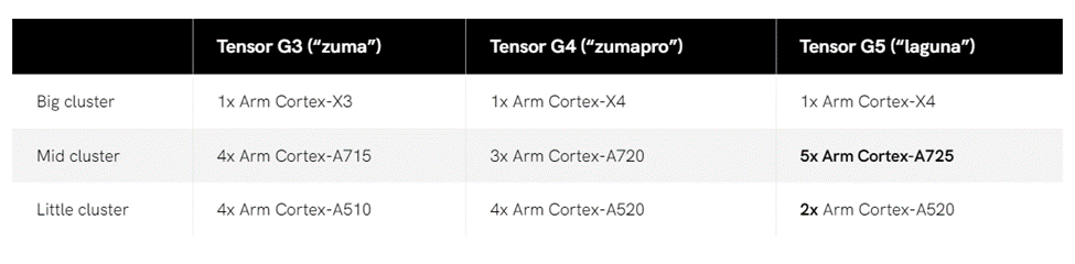
The Tensor G5 will also present upgrades to the CPU cluster.
It will have the same single Arm Cortex-X4 primary core and will shift the core clusters around with five Cortex-A725 cores in the mid cluster and two Cortex-A520 cores in the little cluster.
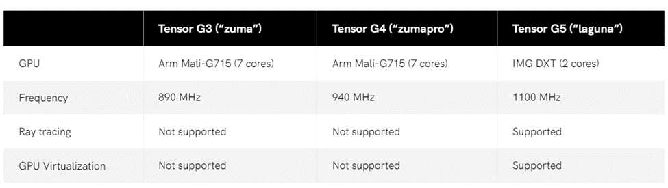
The Tensor G5 comes with a GPU from Imagination Technologies (or IMG) — the DXT-48-1536 running at 1.1 GHz.
The GPU will come with ray tracing support that will be new to Google chips and will provide support for GPU Virtualisation, which will allow accelerated graphics in a virtual machine. Google has been reportedly developing virtualization-based features for some time now.
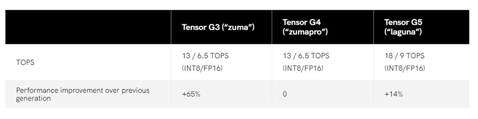
As per the Android Authority report, the Tensor G5 will have a slightly faster TPU than the Tensor G4.
The Trillions of Operations Per Second (TOPS) value is almost 40% larger, while Google’s internal benchmarks suggest the new TPU is only 14% faster.
The advanced TPU will come with small embedded RISC-V cores and support for on-device training.
Tensor G6 On the N3P Node, Set for 2026
The story doesn’t end there as Android Authority was also able to report on the Tensor G6 chip scheduled for 2026.
G6 Chip is codenamed “Malibu” and will be manufactured on TSMC’s next-generation N3P node.
The N3P node is still part of the 3 nm class and introduces some important enhancements to the table. It is rumoured to be used for Apple’s future A19 chip.
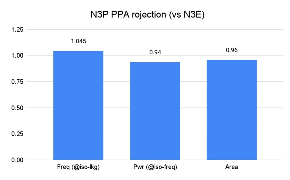
According to the leaked documents obtained by Android Authority, the N3P process node offers the following improvements:
- Frequency (@iso-lkg): A 5% increase allows for higher performance without causing additional leakage (which affects efficiency).
- Power (@iso-freq): A 7% reduction in power consumption when maintaining the same frequency.
- Area: A 4% reduction in the overall size of the chip contributes to a smaller final design.
Android Authority wasn’t able to publish the original leaked documents but managed to recreate the leaked information in this graph –
The technical details may seem complex to layman’s eyes. So, the core takeaway from all the above details is that the Tensor G6 will offer significant gains in performance and efficiency.
It is quite evident that Google is finally stepping up its game with Tensor chips and wants to offer the best technology to its customers. Shifting to cutting-edge nodes, Google is definitely taking steps.
All in all, we can assume that both the upcoming Tensor G5 and G6 chips will offer significant advancements for Google’s processor lineup.
| Feature | Tensor G5 (Laguna) | Tensor G6 (Malibu) |
| Node/Die Size | TSMC N3E, POP packaging, 120 mm2 | TSMC N3P, POP packaging, 113 mm2 current, target 105 mm2 |
| CPU | 1x Cortex-X4, 5x Cortex-A725, 2x Cortex-A520 | 1x Cortex X925 successor (X930), 6x Cortex-A730, 1x Cortex-A530 |
| GPU | IMG DXT 2-core, 1,100 MHz | IMG CXTP 3-core, 1,100 MHz |
| SLC | 8 MB | 4 MB |
| Memory | 4x 16-bit LPDDR5X-8533 or 4x 16-bit LPDDR5-6400 | 4x 16-bit LPDDR5X-8533 or 4x 16-bit LPDDR5-6400 |
| I/O | USB 3.2 Gen2, UFS 4.0, DP1.4, 2x 2 PCIe Gen4 | USB 3.2 Gen2, UFS 4.0, DP1.4, 2x 2 PCIe Gen4 |
| ISP | 200 MP, 108 MP with Zero Shutter Lag, Staggered HDR, 8K 30 video recording | 100x zoom, Cinematic Bokeh engine |
FAQs
Q1. What are the Tensor G5’s process node and expected improvements?
Answer. The Tensor G5 codenamed “Laguna,” will be manufactured on TSMC’s 3 nm-class N3E node, offering significant upgrades in both efficiency and performance.
Q2. What are some of the key features of the Tensor G5?
Answer. The Tensor G5 includes a GPU from Imagination Technologies (IMG), the DXT-48-1536 running at 1.1 GHz, with ray tracing support and GPU Virtualisation.
Q3. What node will the Tensor G6 be built on, and what improvements does it offer?
Answer. The Tensor G6 codenamed “Malibu” will be manufactured on TSMC’s N3P node, offering a 5% increase in frequency, a 7% reduction in power consumption, and a 4% reduction in chip size.
Also Read : Google’s Tensor G5 Chip Reportedly Designed, Set to Power Pixel 10 Series in 2025
Also Read : Google’s Tensor G5 to Use TSMC’s 3nm Process, Enhancing Performance and Efficiency in 2025