Highlights
- Samsung to mass-produce 2nm chips for mobile in 2025, AI and HPC in 2026
- Specialized 4nm node SF4U introduced for better power, performance, and area (PPA)
- Fourth-generation 2nm process SF2Z to feature BSPDN for improved efficiency in 2027
- 3nm SF3E chips already in production, with second-generation SF3 ready for mass production
At this week’s SFF 2024 expo in the US, South Korean semiconductor chip giant Samsung Foundry unveiled its process roadmap for 2nm and 4nm chips, including plans for specialized nodes tailored for AI and automotive applications.
“At a time when numerous technologies are evolving around AI, the key to its implementation lies in high-performance, low-power semiconductors,” said Dr. Siyoung Choi, President and Head of Foundry Business at Samsung Electronics. “Alongside our proven GAA process optimized for AI chips, we plan to introduce integrated, co-packaged optics (CPO) technology for high-speed, low-power data processing, providing our customers with the one-stop AI they need to thrive in this transformative era.”
2nm Samsung Chips Coming Next Year

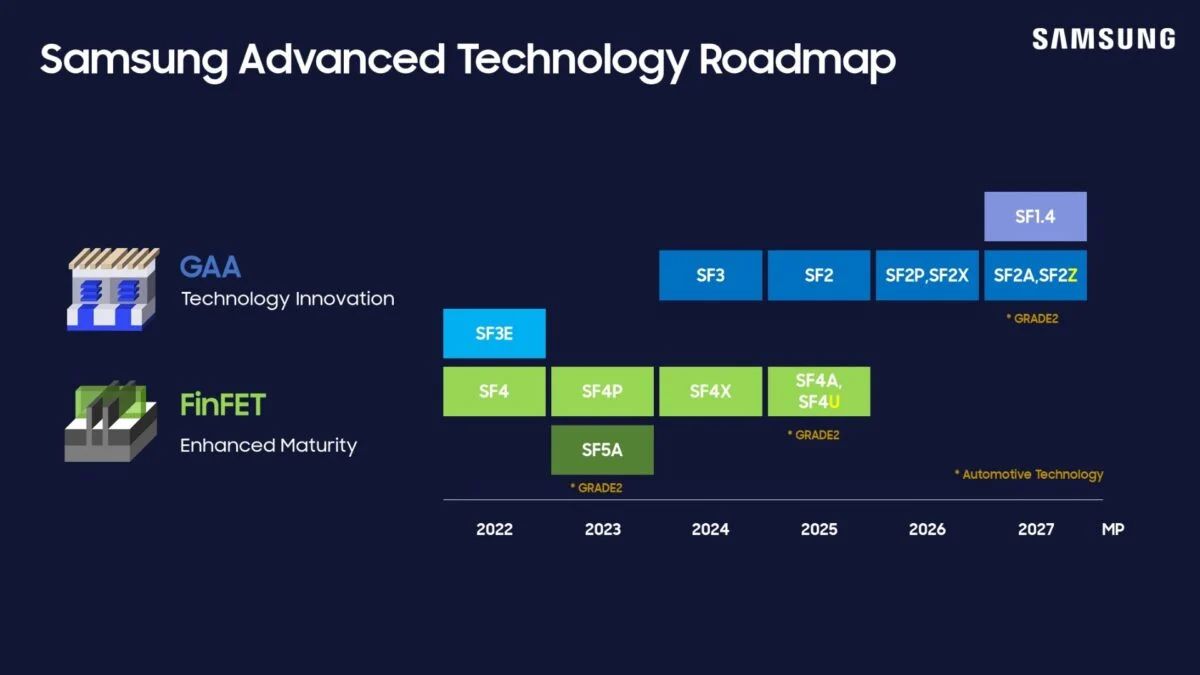
Samsung will mass produce 2nm chips for mobile handsets in 2025.
Its first-generation 2nm process, SF2, is to be ready next year.
An improved one, SF2P, will be ready in 2026.
And a specialized variant, SF2X, that is designed particularly for Artificial Intelligence or AI and High-Performance Computing or HPC and servers will be ready in the same year – 2026.

For the 4nm node, a relatively new type of gas called SF4U was introduced with some optical shrink technology for achieving better power, performance, and area, that is, PPA.
This technology enables existing die designs to be scaled down without significant architectural changes, and mass production is targeted for 2025, primarily focusing on HPC and AI chips.
More Advanced 2nm SoCs in 2027

Also, its fourth generation 2nm process node, SF2Z, will feature BSPDN for better power efficiency as well as temperature control.
In that regard, BSPDN incorporates the use of power rails on the wafer’s backside so as to eliminate any bottlenecks between lines for power and those for signals with mass production set to start in 2027.
Also for automotive chips, a derivative of the 2nm process, SF2A, is to enter into mass production in 2027.

Samsung claims its GAA transistor architecture introduced with its 3nm process is maturing continuously, improving performance and yield levels, and the company will apply the design to its 2nm stages as well.
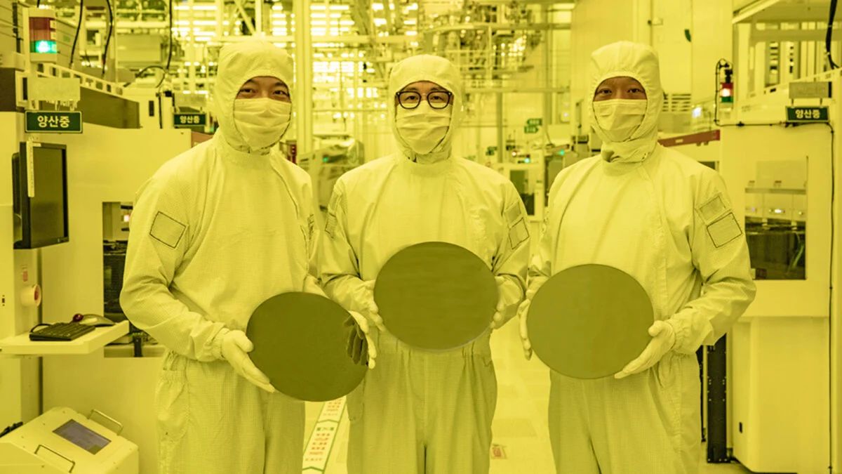
While Samsung started mass-producing 3nm (SF3E) chips in the second half of 2022, primarily for cryptocurrency mining chips, its second-generation 3nm process, dubbed SF3, is now ready for mass production.
Reports suggest that Samsung’s own Exynos W1000 might be the first chip to utilize this technology, although the company did not provide specific details during the event.
FAQs
When will Samsung’s 2nm chips be available for mass production?
Samsung plans to start mass-producing 2nm chips for mobile devices in 2025, with specialized variants for AI and HPC ready by 2026.
What is the SF4U node introduced by Samsung?
The SF4U node is a 4nm process featuring optical shrink technology to improve power, performance, and area (PPA), enabling existing die designs to be scaled down without significant architectural changes.
What advancements will the fourth-generation 2nm process SF2Z offer?
The SF2Z process will incorporate BSPDN technology for better power efficiency and temperature control, with mass production targeted for 2027.
What applications will benefit from Samsung’s new 2nm and 4nm chips?
The new 2nm and 4nm chips are designed for a variety of applications, including mobile devices, AI, high-performance computing (HPC), and automotive sectors.
Also Read: Samsung Exynos 2400: The Rumoured Deca-core Revolution in Smartphone Processing
Also Read: Samsung Exynos Gets New SoCs; Details Inside
